Page 2 of 11
Re: Another Home-Brew - Z180
Posted: 01 Sep 2019 13:10
by 1024MAK
Or use an expanded RC2014 backplane (see
here for a selection).
Mark
Re: Another Home-Brew - Z180
Posted: 07 Sep 2019 22:06
by Bill B
Attached is the proposed circuit diagram for a cut down board, just CPU and memory. The UART built into the Z180 means that this board will be testable as-is. This design includes an edge connector with the minimum signals required for I/O expansion, assuming just 8-bit I/O addresses.
Using an EPM7128 CPLD for this would be over-kill. Fortunately, amongst the chips Lez sent me were some smaller EPM7032 versions.
The EPM7032 chips do not have enough pins for all the address lines required and eight data lines. Fortunately, I only need a four bit register for the ROM mapping I am planning:
- 0000b = Linear mapped Flash ROM, read only (default after reset).
- 0001b = Linear mapped Flash ROM, read / write.
- 0100b = No ROM, all RAM.
- 1xxxb = Banked ROM, bank xxx.
One other change from the original design. The spec for the Z180 clock signal is:
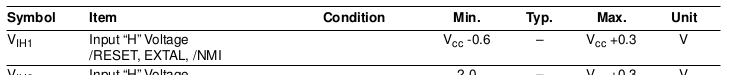
- Z180_DC_Spec.png (10.58 KiB) Viewed 9312 times
So a minimum high level of 4.4V. However the output drive characteristics of the CPLD are:
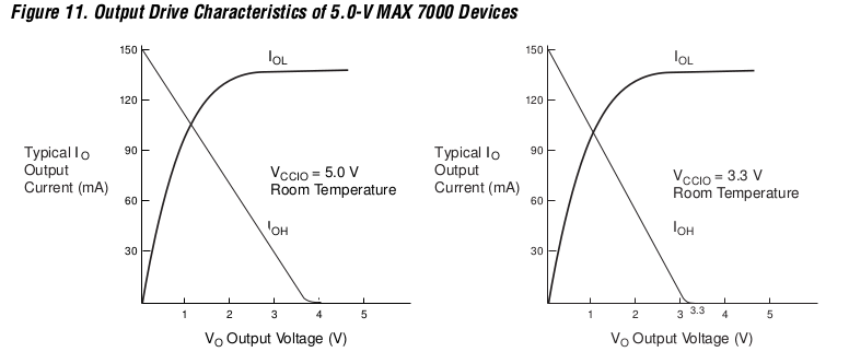
- MAX7000_Drive.png (42.68 KiB) Viewed 9312 times
So even at zero output current, the maximum high voltage is only 4.0V. Thus the CPLD is out of spec as a clock source for the Z180. I will therefore attach the oscillator module directly to the Z180 chip. I will socket it to make it easy to put a different frequency module in instead. It would be possible just to use a crystal, since the Z180 has a built in oscillator, but that would require a slightly different PCB layout.
I may be being unnecessary cautious here, as I believe that Dave and Martin run the MTX+ clock through a CPLD.
One change to the attached circuit diagram that I am contemplating is to use the remaining spare pin on the CPLD as Write Enable for the Flash ROM, rather than just attaching the Write Enable to Z180 Write. That would allow the Flash ROM chip select to go active as soon as the relevant address range is selected, rather than having to wait until RD is asserted.
The draft VHD for the CPLD is:
Code: Select all
library ieee;
use ieee.std_logic_1164.all;

entity  Z180_EC_Mem_CPLD is
  port (
    data : inout std_logic_vector(3 downto 0);
    addr_lo : in std_logic_vector(7 downto 0);
    addr_hi : in std_logic_vector(19 downto 14);
    rd, wr, mreq, iorq, reset : in std_logic;
    addr_rom : out std_logic_vector(16 downto 14);
    cs_rom, cs_ram0, cs_ram1 : out std_logic
    );
end Z180_EC_Mem_CPLD;

architecture behaviour of Z180_EC_Mem_CPLD is
  constant port_mmap : std_logic_vector(7 downto 0) := X"40";
  signal mmap : std_logic_vector(3 downto 0) := ( others => '0' );
  signal sel_rom : std_logic := '1';
begin
  -- Memory mapping
  process (iorq, wr, addr_lo, data)
  begin
    if ( reset = '0' ) then
      mmap <= ( others => '0' );
    elsif ( ( iorq = '0' ) and ( wr = '0' ) and ( addr_lo = port_mmap ) ) then
      mmap <= data;
    end if;
  end process;
  addr_rom <= mmap(2 downto 0) when ( mmap(3) = '1' ) else
              addr_hi (16 downto 14);
  sel_rom <= '0' when ( mmap(3) = '1' ) and ( addr_hi = "000000" ) else
             '0' when ( mmap(3) = '0' ) and ( mmap(2) = '0' ) and ( addr_hi(19 downto 17) = "000" ) else
             '1';
  cs_rom <= mreq or sel_rom or ( rd and not mmap(0) );
  cs_ram0 <= mreq or addr_hi(19) or ( not sel_rom );
  cs_ram1 <= mreq or ( not addr_hi(19) );
  -- Buffered data
  data <= mmap when ( ( rd = '0' ) and ( iorq = '0' ) and ( addr_lo = port_mmap ) ) else
          ( others => 'Z' );
end behaviour;
Next task is to see whether I can route this cut-down board at a reasonable size. I also need to check that I can assign each of the functions to the pins that I want to.
Re: Another Home-Brew - Z180
Posted: 09 Sep 2019 19:50
by Martin A
That's an interesting discovery. Tony's flexible clocking system for the MTX plus uses the EPM7128.
That's driving the clock on the Z80 (and everything else), which has the same input spec as the Z180.
And it works, even though perhaps it shouldn't, maybe it's a good thing I'd not read that part of the datasheet!
I put the scope on the clock signal it's registering about 3.7v or so. That's driving a Z80 and a CTC and a backplane. Both seem to be happy with the output of the CPLD.
The CPLD seems to be working to spec, the 0.3 drop seems to match the graph since both devices are CMOS there won't be a heavy load.
The Zilog devices, on the other hand, it seems are better then the spec suggests.
Re: Another Home-Brew - Z180
Posted: 09 Sep 2019 21:30
by Bill B
Just looking back at the MTX circuit diagram in the manual. It uses the six inverters in a 74S04 chip as the clock source. Three of the inverters are used as output drivers, one for the CPU, one for the CTC and one for everything else, The CPU and CTC drivers each have 330R pull-ups to 5V, presumably in order to meet the clock high spec. That does mean that each of these inverters are sinking ~15mA at clock low !
Re: Another Home-Brew - Z180
Posted: 09 Sep 2019 22:24
by 1024MAK
A failure of a Z80 to accept a clock has been seen elsewhere (not that I can remember where mind) when driven with a normal 74LSxxx part.
And Sinclair used a transistor with a 180Ω to 330Ω pull-up resistor to buffer the ULA clock output to the NMOS Z80A in their ZX81 and ZX Spectrum models.
Mark
Re: Another Home-Brew - Z180
Posted: 15 Sep 2019 09:34
by Bill B
As suggested earlier, I have revised the circuit diagram to have a separate ROM Write Enable signal.
The revised VHDL for this is:
Code: Select all
library ieee;
use ieee.std_logic_1164.all;

entity  Z180_EC_Mem_CPLD is
  port (
    data : inout std_logic_vector(3 downto 0);
    addr_lo : in std_logic_vector(7 downto 0);
    addr_hi : in std_logic_vector(19 downto 14);
    rd, wr, mreq, iorq, reset : in std_logic;
    addr_rom : out std_logic_vector(16 downto 14);
    cs_rom, cs_ram0, cs_ram1, wr_rom : out std_logic
    );
end Z180_EC_Mem_CPLD;

architecture behaviour of Z180_EC_Mem_CPLD is
  constant port_mmap : std_logic_vector(7 downto 0) := X"40";
  signal mmap : std_logic_vector(3 downto 0) := ( others => '0' );
  signal sel_rom : std_logic := '1';
begin
  -- Memory mapping
  process (iorq, wr, addr_lo, data)
  begin
    if ( reset = '0' ) then
      mmap <= ( others => '0' );
    elsif ( ( iorq = '0' ) and ( wr = '0' ) and ( addr_lo = port_mmap ) ) then
      mmap <= data;
    end if;
  end process;
  addr_rom <= mmap(2 downto 0) when ( mmap(3) = '1' ) else
              addr_hi (16 downto 14);
  sel_rom <= '0' when ( mmap(3) = '1' ) and ( addr_hi = "000000" ) else
             '0' when ( mmap(3) = '0' ) and ( mmap(2) = '0' ) and ( addr_hi(19 downto 17) = "000" ) else
             '1';
  cs_rom <= mreq or sel_rom;
  cs_ram0 <= mreq or addr_hi(19) or ( not sel_rom );
  cs_ram1 <= mreq or ( not addr_hi(19) );
  wr_rom <= mreq or sel_rom or wr when ( mmap = "0001" ) else '1';
  -- Read back memory map
  data <= mmap when ( ( rd = '0' ) and ( iorq = '0' ) and ( addr_lo = port_mmap ) ) else
          ( others => 'Z' );
end behaviour;
I have confirmed that Quartus will compile that, with the signals assigned to the pins I want. It reports 23 / 32 (72%) of macrocells used.
I am able to fit this circuit onto a Eurocard size board (160 x 100mm), see the attached PDF. The fit is fairly tight, with room for mounting holes in only three of the four corners.
Before comiting this layout to copper, I will check the design of the peripherals board.
Re: Another Home-Brew - Z180
Posted: 15 Sep 2019 15:14
by Martin A
Is it worth feeding 0v to the 2 no connects on the rom socket, just in case you need to fit a larger Flash in there for any reason.
Or jumper them for either voltage to allow for multiple rom images ??
Re: Another Home-Brew - Z180
Posted: 15 Sep 2019 15:18
by Bill B
Good point Martin, I will see what I can fit in.
Re: Another Home-Brew - Z180
Posted: 15 Sep 2019 22:26
by Bill B
Added the ROM address jumpers as suggested by Martin. A bit of a squeeze to fit them onto the PCB without moving everything.
Not sure that I will need them. My present thought is that the ROM will just contain a boot loader, and everything else will be loaded from SD card. It makes development easier. So even a 16KB ROM would probably be ample.
However once the code is firmed up, there might be advantages to moving BIOS & BDOS type code onto ROM.
Re: Another Home-Brew - Z180
Posted: 22 Sep 2019 17:00
by Bill B
My first attempt at constructing the CPU PCB failed. I attempted to use a piece of PCB which I have had for too many years. The photo-resist has obviously got old, and relatively insensitive to UV.
- Failed_PCB.jpg (87.35 KiB) Viewed 9224 times
During development the etch-resist has failed to come completely away from the copper. The other side is even worse, with the tracks faded out in numerous places.
Two lessons to be learnt:
- Don't buy more photo-resist PCB than you expect to use, as it does not keep. Unfortunately P&P costs tend to encourage over buying,
- Get a piece of board slightly bigger than needed, and use the off-cuts for exposure testing before trying to make the main board. I did actually do an exposure test, but that was on a bit of single sided board which was clearly not of the same vintage.
If I clean off all the old photo-resist from this board, I think I have three options for reusing it:
- Spray-on photo-resist. This needs to be applied in a darkroom.
- Amazon offers photosensitive dry film. I have never tried this, but looks complicated and requires a negative image.
- Thermal transfer of toner onto the PCB. I have tried this a couple of times without much luck.
I will probably just buy some new photo-resist PCB.