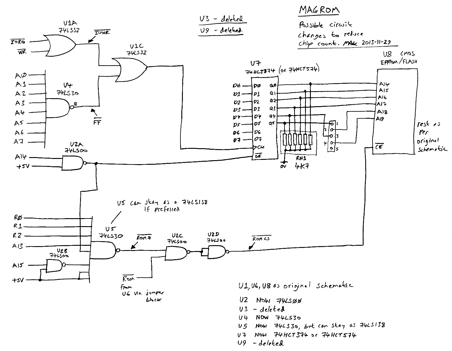
Okay, this draft amendment schematic reduces the chip count by two

.
U1, U6, U8 stay the same type (but U1 and U8 have some wiring changes) as per Martin's schematic.
U2 has now been changed to a 74LS00 NAND chip.
U3 has been deleted.
U4 has now been changed to a 74LS30 NAND chip.
U5 has now been changed to a 74LS30 NAND chip, but if preferred can stay as a 74LS138 (just use Martin's schematic).
U7 has now been changed to a 74
HCT374 or a 74
HCT574 (these both provide the same function, but have different pin-outs).
U9 has been deleted.
RN1, a 4.7k resister network has been added (7 pin 6 resistor network or larger). Normal resistors can be used instead.
- MAGROM_mods_draft(50).png (226.3 KiB) Viewed 37804 times
As the latch now used (U7) does not have a clear/reset input, the "firmware" running in "ROM7" (address block 02000h to 03FFFh)
of the EPROM/FLASH (U8) should make sure that the correct value is latched before accessing the EPROM/FLASH (U8) as "RAM".
There is no problem accessing the correct address range when the EPROM/FLASH (U8) is accessed as "ROM7" (address block
02000h to 03FFFh), as when address line A14 is low, U2A inverts this signal and it is applied to the three state /OE input of the latch
(U7) which disconnects the outputs and puts them into a high impedance condition. This allows resistor network (RN1) to pull down
the address lines A14 to A19 of the EPROM/FLASH (U8) selecting the lower memory block.
Hopefully my brain was fully operational when I doodled this and I have not made any logic (or other!) errors. Feel free to shout out
if I have dropped a boo-boo
 Mark
Mark