Page 1 of 1
MTX Serial port schematic
Posted: 07 Mar 2014 13:16
by JonB
hi
Has anyone got a schematic of the MTX serial card? I am thinking of recreating it as a little project, seeing as how they are pretty rare in the wild.
Also, how does it interface to the bus? I am assuming it's addressed via the Z-80's I/O port map (so, for example, OUT (n),A would be used to transmit rather than via a memory mapped register as you do with the 6502). Of course, I can deduce this from the schematic - and does the MTX have the firmware support already built into the ROMs?
To be fair, it doesn't look very complicated (from the electronic perspective) from the picture on Andy's site:
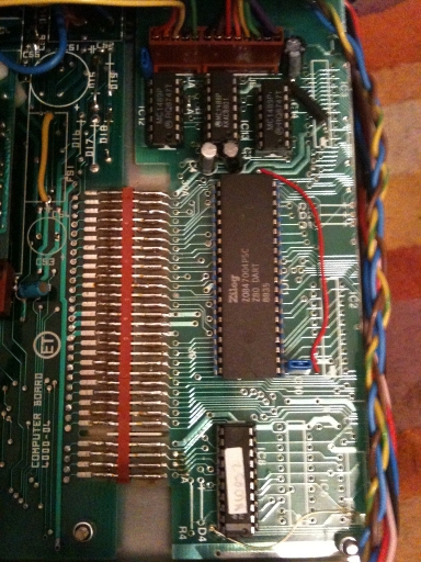
I see a Z80 DART chip, a set of three MC1489 line driver/receivers and a logic chip (which I can't identify).
Cheers
JonB
Re: MTX Serial port schematic
Posted: 07 Mar 2014 13:49
by Dave
Well, as they say, "you can lead a horse to water . . . . ." <sigh>
Have you checked my Manuals page ?
http://www.primrosebank.net/computers/m ... anuals.htm
A good place to look might have been the "MTX500/512Service and Technical" Manual
There is also a pointer to the circuit diagrams in the "Phoenix Operators Manual"
And also the "FDX Technical Manual"
The latter has the clearest copy of the RS232 board schematic, scanned from my original
http://www.primrosebank.net/computers/m ... htm#fdx_tm
regards
Dave
Re: MTX Serial port schematic
Posted: 07 Mar 2014 15:54
by JonB
Thanks Dave, I didn't think to look in the FDX manual. I did check the page though (first port of call!) but I skipped over the FDX.
Hmm, the logic chip seems to be a PLA (which I don't know a lot about!). It's supplying !DARTEN by the looks of it. I can't make much sense of the diagrams - they are for the full on comms board (with FDX header) rather than the chopped off serial only board linked to above. But that chip at the bottom is IC8 which is the PLA. This should be recreatable in discrete logic, if I can find out how it is configured.. anyone got any ideas?
Re: MTX Serial port schematic
Posted: 07 Mar 2014 17:02
by Martin A
The PAL equations for the serial port are on Pg249 of the "Phoenix" manual.
They're for the Full RS232 and interface, but I doubt the DART enable changed for the RS232 only card.
/darten = /A7 * /A6 * /A5 * /A432 * /IORQL * M1L
A432 is formed on the RS232 board (4 input NAND IC9?) and is low when A2 and A3 are high and A4 is low
The dart needs to be paged in for IORQ low, M1 high, and port address in the range 0CH to 0FH
For discrete logic maybe a 74xx138 and a couple of OR gates ought to do it. One of M1,A2 or A3 as the active high enable onthe 138, OR together any 2 pairs of the low signals to the active low enables ( out of A7,A6,A5,A4 and IORQ), and the remaining 2 high and 1 low signals get fed to the ABC inputs, depending how they're wired one of the Y outputs (from Y3 Y5 or Y6) is your /darten signal
Re: MTX Serial port schematic
Posted: 07 Mar 2014 17:22
by JonB
Hi Martin, thanks for replying so soon.
What do the asterisks in your boolean formula mean? AND, I guess.
Also, there doesn't appear to be an IC9 on the photo I posted of the chopped off FDX card. So maybe this is another function of the PLA, or am I missing something?
Cheers
JonB
Re: MTX Serial port schematic
Posted: 07 Mar 2014 19:30
by 1024MAK
JonB wrote:What do the asterisks in your boolean formula mean? AND, I guess.
Also, there doesn't appear to be an IC9 on the photo I posted of the chopped off FDX card. So maybe this is another function of the PLA, or am I missing something?
Jon
Yes the asterisks mean AND.
It is very likely that the PAL on the cut-down serial board has a different formula, hence the extra logic gate is not needed.
The logic you require is:
Code: Select all
DART I/O address
      <address>
Hex   7654 3210
0C =  0000 1100
0F =  0000 1111
So the selection logic needs to have an active low (to enable the DART) when A2, A3 and /M1 are high and when /IORQ, A4, A5. A6 and A7 are low. Note that as far as the decoding goes, A1 and A0 are don't care, as these are inputs to the DART chip.
If you want a one chip, "standard" logic solution, use a 74HCT688 8-bit equality comparator (see
here for easy links to data sheets

Wire the eight inputs to one set (group) of inputs (say inputs P0 to P7), then wire the corresponding second input pin (Q0 to Q7) to either +5V for logic 1 (high) or 0V for logic 0 (low) depending on whether the input on the "P" input is a 0 or 1.
So for example, if you route A2 to the P0 input, wire the Q0 input to +5V. The output pin /(P=Q) can then be fed to the enable pin (/CS) on the DART.
Mark
Re: MTX Serial port schematic
Posted: 08 May 2014 17:32
by thewiz
Just added a new topic basically asking what you are looking to do. Sigh! Did you get any futher with this?
My use would be to connect my MTX to my PC for data transfer.
Regards
Re: MTX Serial port schematic
Posted: 12 May 2014 14:45
by JonB
No, but since I have a Remorizer now, I don't really need serial... I will follow your new thread with interest, though!