- PCB_Detail.png (75.57 KiB) Viewed 18727 times
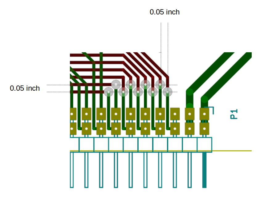
I am going to have to re-think my PCB designs again. With a home made PCB it is necessary to solder small pieces of wire between the upper and lower pads of a via. My soldering is not good enough to do this between pads at 0.05 inch spacing without creating shorts between pads or tracks. It does not help that my UV box is single sided. It is very difficult to keep alignment between the upper and lower layers as I turn the board over. I did quite well with the CPU board, not so well (~1mm out) with the Peripherals board.
Dave is undoubtedly right, it would be more reliable and higher quality to have the boards made professionally. By the time you count wasted materials, broken drill bits and effort taken, probably cheaper and quicker as well. But it seems a shame to have the tools and not use them. Also the "I made that" satisfaction.
One option is to do single sided boards and use wire links instead of tracks on the upper layer. It will still be necessary to move the via pads further apart (0.1 inch spacing) in order to be able to solder the links to the tracks without shorts. Ideally I would like to be able to make the via pads rectangular, but would then need to be able to orient them horizontal or vertical. And with the extra spacing, possibly a double layer board will work.
Back to the drawing board

