Hello, I think I'm due for an update, sorry for such delay, but better late than never.

To recap what has been done:
-One of video RAM chips (4116) was bad and it was replaced
-C11 was replaced but had a cold solder joint, symptoms: after a while the computer went into a "reset loop", on screen the signal (video output) could be seen for a fraction of a second. Resolution: fixed the cold joint on C11
-After the reset issue was fixed the image was "stable/persistent", however after a couple of seconds the image got weird artefacts (see Image) covering the whole screen.
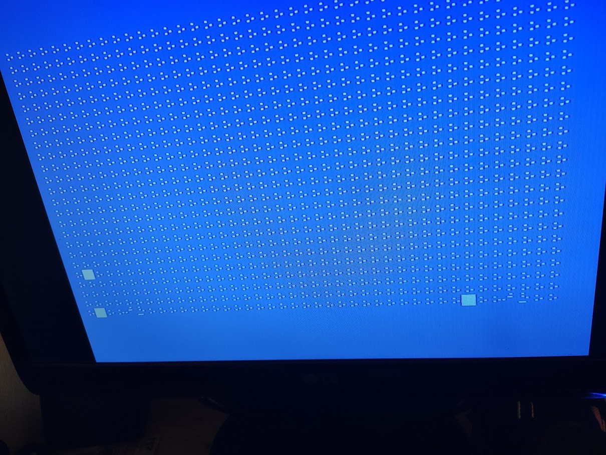
- IMG_20210328_111430.jpg (264.37 KiB) Viewed 23325 times
-At this stage I wanted to see what happened if I run a Basic program (simple print loop), however trying to type it in I noticed that some of the keys were dead. I checked the continuity on keyboard and connected logic etc.... Checking the keyboard matrix I noticed that all of the nonworking letters were on the same line, this lead me to changing the 74LS273 at 3A, which fixed the dead letters and allowed me to type in a print loop. I left the loop running for 1h and the screen was fine (without artefacts) this lead me to believe the computer was generally working and that the artefacts are caused by the input part and the video RAM/display part was fine.
At this stage I swapped the 74LS244 at D1, C1 and E2 this gave me a stable basic prompt. (I only recently got TL866II Plus that will enable me to test which chip was faulty) I was dealing with fake Chinese LS244 in between that's why I swapped all 3 of them and I was a bit desperate

. Interchanging 74xx244 between sockets, produced similar image, just the pattern was a bit different (hopefully someone will find this information useful).
At this point I switched the Link 6 and link 7 to 512 configuration, but the computer at this stage booted to black screen, after some inspection of the PAL14L4 extension board (timing fixing board) I noticed a cold solder joint on one of the pins. After a fix the computer boots to basic.
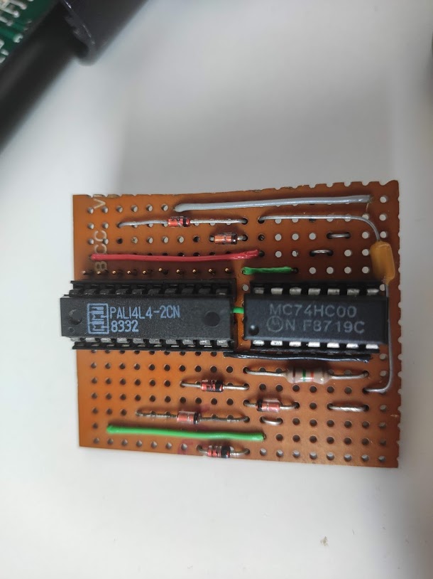
- IMG_20210605_142522.jpg (65.05 KiB) Viewed 23325 times
I had some issues loading software (because of using stereo cable, stupid I know
) which led me to study the timing correction board a bit. The result is the attached schema of it. It's basically an logical AND operation (over multiple NAND gates, 74HC00 logic chip) between pin 14 on PAL14L4 chip and pin 2, 4, 7 and 18. I checked the continuity of the board but all was fine, then I realized the cable I was using was stereo
.
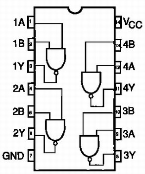
- Ext-2201-000.jpg (26.48 KiB) Viewed 23325 times
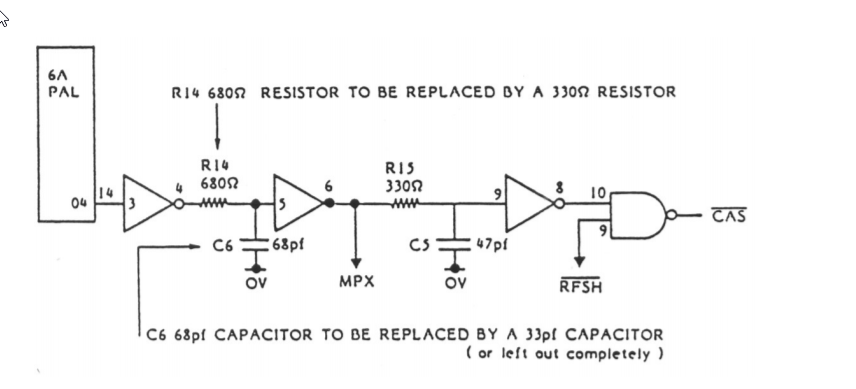
- unnamed.png (88.69 KiB) Viewed 23325 times
After making a mono cable everything seems to work fine and I'm very happy to save this wonderful part of computer history.
It was an epic struggle (mainly because the Chinese poste, COVID delays and my learning process), but worth it and I really appreciate all of the help and feedback from the wonderful community.
Have a nice day and thanks for all the help.

